#mcu csr interface
Explore tagged Tumblr posts
Visit Tumblr Blog
Explore Tumblr blogs with no restrictions, modern design and the best experience.
Last Seen Tumblr Blogs


Fun Fact
Tumblr’s website traffic is steadily declining.
Photo
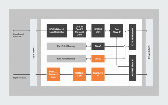
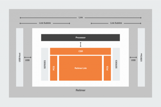
USB 3.1 Appendix E standard-USB 3.2 Retimer
We offer USB IP subsystem, FPGA boards, SERDES interface, USB 3.1 Device Controller, USB 3.2 Retimer, SRIS architecture, MCU CSR interface.
#USB 3.1 Appendix E standard#usb 3.2 retimer#usb ip subsystem#fpga boards#serdes interface#mcu csr interface
0 notes
Text
Wireless USB Bluetooth 5.0 Adapter Transmitter Music Receiver Mini BT5.0 Audio Adapter for Computer PC Laptop Tablet
Wireless USB Bluetooth 5.0 Adapter Transmitter Music Receiver Mini BT5.0 Audio Adapter for Computer PC Laptop Tablet
Just For Today
Just For Today get free read 60 days !!!
Only At My Best Shop Place : https://s.click.aliexpress.com/e/_AExmqU
Wireless USB Bluetooth 5.0 Adapter Transmitter Music Receiver Mini BT5.0 Audio Adapter for Computer PC Laptop Tablet

Description: 5.0 Bluetooth dual-mode dongle, compatible with Bluetooth 2.1, 3.0, 4.0, 4.1 and 4.2 specifications. The chip integrates a low-power MCU, RF transceiver, baseband, modem, USB, UART, PCM / I2S, SARADC and 24 GPIOs with the Berry Bluelett protocol stack to provide low-cost, low-power flexible and powerful Bluetooth application Support Cass1 / 2 Power level Supports Bluetooth 5.0 dual-mode specifications, supports both classic Bluetooth and Bluetooth low energy Support USB / UART Support 7-BR / EDRE ACL link, 1-SCO / eSCo audio link and 1- BLE slave link or 4- BLE master Working temperature -20 to 70 ℃ Supported operating systems: for Windows, for Android, for Linux, for FREERTOS, for ThreadX UITRON Support software: for Bluetooth software, CSR Harmony, Bluez, Bluesol eil. Bluelet. Bluedroid Support application functions: for HFP / HSP (hands-free phone / headset) A2DP / AVRCP (stereo music) HID / HOGP (keyboard and mouse). DUN / PAN (Internet access), PBAPMA PFTPSPP.GATT, etc. Description: Item Name: V5 Bluetooth 5.0 Adapter Interface: USB Transfer rate: Max 24Mbps Bluetooth Version: Bluetooth V5.0 Frequency Band: 2.400-2.480GHz Pr transmit power: + 10DBM (Class II) Sensitivity: -90dBm 0.1% Speed: 3Mbps Color: Black Item Size: 21x16x5 mm Support system Windows XP / Vista / Win7 / Win8 / Win8.1 / Win10.
0 notes
Text
MCU CSR Interface-Interlaken Protocol and Ethernet Protocol-ASIC/SoC Physical Design
The multi-control framework is executed in this paper. Being happy with the prerequisites for Bluetooth profile determination and concentrating on the part to be improved, the method for an original application is presented. MCU CSR interface depends on Bluetooth sequential port profile, by utilizing CSR BC02 and MCU, a multi-control framework application is carried out. In light of the exploration of Bluetooth Protocol, a sort of Bluetooth information moving framework given MCU-controlling has been proposed in the paper. In the framework, the MCU where the Bluetooth HCI convention has been implanted is utilized to control the Bluetooth module on UART and make the Bluetooth gadgets in the Bluetooth network set up an association and move information naturally.
In the equipment plan, the chip C8051F020 is chosen as the host regulator. There are many fields and conditions to be checked in the HIRFL-CSR control framework. The field clever gear in light of MCU is planned, the framework functional standard, equipment setup, and programming block graph exile, and the capacity of the screen framework and its strategy for acknowledgment are portrayed. The framework enjoys benefits like a cordial point of interaction, the minimal expense of plan and basic activity, and acceptable experimental outcomes have been accomplished.
Interlaken protocol and Ethernet protocol are two principal structures that characterize the Interlaken Protocol the information transmission design and the Meta Frame. The information transmission design depends fundamentally on the ideas of SPI4. Information sent across the interface is fragmented into explodes, which are subsets of the first bundle information. Each burst is limited by two control words, one preceding and one after, and sub-fields inside these control words influence either the information following or going before them for capacities like beginning of-parcel, end-of-bundle, blunder recognition, and others.
Each burst is related to an intelligent channel, which can address a physical systems administration port in the framework or another sensibly associated stream of information. Parcel information is sent successively through at least one explodes, and the size of the blasts is a configurable boundary. By fragmenting the information into explodes, the interface permits the interleaving of information transmissions from various channels for low-inactivity activity. The Meta Frame is characterized to help the transmission of the information over a framework. It envelops a bunch of four interesting control words, which are characterized to give path arrangement, scrambler introduction, clock remuneration, and indicative capacities.
The last segment of this paper diagrams procedure that is empowering the SoC plan at these levels. A further developed ASIC/SOC physical design plan philosophy for fast plan intermingling is depicted in this paper. Not at all like the customary ASIC/SOC plan strategies zeroed in on mechanization, our new strategy centers around smoothing out the ASIC/SOC stream's planning-consuming strides by applying our master's BKM's (most popular system) to speed up plan combination.
integrated circuits (ASICs) and system-on-a-chip (SoC) plans. This procedure is utilized by both IBM ASIC and SoC planners, just as OEM clients. A vital focal point of the IBM ASIC/SoC procedure, illustrated in the primary segment of this paper, is the initial time-right strategies for plan and confirmation that boost the right activity of the chip upon item incorporation. The second part of this paper depicts progress in an approach that arrangement with the actual impacts of contracting gadget calculations and empower configuration utilizing the presentation and thickness capacities accessible in the new advances, and systemic advances that have further developed plan turnaround time (TAT) for huge, complex plans. Impending nanometer-level advancements present new chances to incorporate frameworks on a solitary chip, including practical parts of blended libraries and blended simple and computerized plans. It empowered us to abbreviate the tedious stages drastically with generally negligible exertion. --
0 notes
Text
HBM 3D-stacked DRAM Technology-MCU CSR Interface-SERDES Interface
As of late, the HBM 3D stacked DRAM technology, which is known as HBM (high data transfer capacity memory), utilizing the TSV interaction has been created. The stacked memory structure gives expanded data transmission, low power utilization, just as little structure factor. There are many plan difficulties, for example, multi-channel activity, miniature knock test, and TSV association check.
HBM (High Bandwidth Memory) is an arising standard DRAM arrangement that can accomplish advancement transmission capacity of higher than 256GBps while lessening the power utilization also. It has a stacked DRAM design with center DRAM bites the dust on top of a base rationale pass on, in view of the TSV and pass on stacking innovations. In this paper, the HBM design is presented and a correlation of its ages is given.
Additionally, the bundling innovation and difficulties to address dependability, warm dispersal capacity, greatest admissible bundle sizes, and high throughput stacking arrangements are depicted. Different plan strategies make it conceivable to conquer the troubles in the advancement of TSV innovation. Vertical stacking empowers more different memory engineering than level design.
Bluetooth Protocol, a sort of Bluetooth information moving framework dependent on MCU-controlling been proposed in the paper. In the framework, the MCU CSR interface wherein the Bluetooth HCI convention has been inserted is utilized to control the Bluetooth module on UART and make the Bluetooth gadgets in the Bluetooth network set up an association and move information naturally. In the equipment plan, the chip C8051F020 is chosen as the host regulator. Since chip C8051F020 has two UART sequential interfaces, it can meet the prerequisite of configuration, work on the circuit and improve framework hostile to sticking capacity.
The multi-control framework is carried out in this paper. Being happy with the necessities for Bluetooth profile particular and concentrating on the part to be improved, the methodology for a clever application is presented. This paper depends on Bluetooth sequential port profile, by utilizing CSR BC02 and MCU, a multi-control framework application is executed. Modern creation regularly experiences issues in refreshing the program of MCU(Micro Controller Unit), and the cycle boundaries cannot be refreshed on a case-by-case basis continuously.
As the proposed LC-VCO is planned to be amazingly adaptable without overhaul for quite a long time age SERDES interface, a wide working recurrence makes the stage locked circle (PLL) pertinent to the multistandard. To show a profoundly aggressive plan, a quality (Q) factor upgrade method has been additionally shown to decrease the misfortune from the dynamic inductor, prompting a suitable stage commotion over the whole tuning range.
To work with the internet-based updates of the STM8 microcontroller, the paper planned an STM8 online downloader dependent on the STM32 microcontroller and SWIM convention. The downloader doesn't depend on a PC or a committed download gadget. It has a basic circuit structure and is not difficult to download on the web, precisely, and fast. At the point when STM32 associates with a touch screen, the downloader can change boundaries on the web.
Ongoing 3D-stacked in-bundle memory gadgets like high-transfer speed memory (HBM) and comparative advancements can give high measures of memory data transmission at low access energy. Nonetheless, 3D-stacked in-bundle memory has a restricted memory limit. In this paper, we study and present the difficulties of scaling the limit of 3D-stacked memory gadgets by stacking more DRAM kicks the bucket inside a gadget and building taller memory stacks. We likewise present possible bearings and alleviations to building tall HBM heaps of DRAM bites the dust.
Albeit taller stacks are a conceivably intriguing way to deal with increment HBM limit, we show that more exploration is expected to empower high-limit memory stacks while at the same time increasing their memory data transfer capacity. In particular, elective holding and stacking advancements can be researched as a possible major empowering influence of tall HBM stacks.
These distinctions bring about varieties in trademark impedance and engendering speeds, which might be negative at high information rates. The inclusion misfortune (IL), inside pair slant, and differential to normal mode change proportion of transmission lines may radically increment because of the fiber weave impact. Thus, the connection financial plan of rapid correspondence channels might be fundamentally ruined. This resolves the issues because of the fiber weave impact and gives moderation strategies at the bundle level, especially for the 56 Gbps Serializer/Deserializer (SerDes) interface. With fast IO interfaces moving toward Terabit data transmission, multilane SerDes (serialize/deserialize) IO designs become promising.
By putting high-velocity sequential information joins in equal, the IO interface transfer speed is altogether expanded. The design, nonetheless, has forced a few difficulties underway testing. On one hand, the conventional piece mistake rate test can't be cost-successfully conveyed with gigantic measures of SerDes put in equal. Then again, a basic loopback test doesn't give sufficient test inclusion to simple execution varieties. In satellite frameworks, a lot of high-velocity information is needed to be sent starting with one framework then onto the next.
Customary equal information transmission requires countless links/interface bundles and results in enormous weight and volume. Equal interface in a common future camera framework requires >8000 links between camera hardware and information dealing with the framework. Furthermore, with an expansion in transmission rate, issues related to crosstalk become more basic. One potential arrangement distinguished is the sequential interface, additionally named as SERDES (Serializer/DESerializer) interface.
A regular SERDES interface contains encoder/decoder, PLL, timing-control, and multiplexer/de-multiplexer. Encoding of sequential information settles high-velocity sequential information transmission issues by fusing clock installing, DC adjusting, sync data addition, and mistake discovery. DC adjusting likewise tackles the issue of Inter-Symbol Interference (ISI). Accessible SERDES interface gadgets have restrictions like helpless decrease factor, no clock inserting, or non-accessibility of the space-qualified parts. Consequently, an endeavor is made to comprehend and execute this interface with the objective of native SERDES ASIC advancement, which will likewise conquer the above issues.
Different sequential encoding strategies are studied and an 8B/10B encoding method is concluded for exceptionally fast sequential information transmission. As an underlying advance, an 8B/10B encoding-based SERDES interface is executed in an FPGA. Consequently, SerDes can be an extraordinary arrangement in moving huge information from direct A toward Point B inside the framework, between two distinct frameworks, or without a doubt between frameworks in better places. SerDes permits information to be sent at a higher rate and is more affordable. In this paper, the plan, and confirmation of SerDes have been proposed. Verilog HDL was utilized in the plan of SerDes and confirmation was done utilizing Universal Verification Methodology (UVM) as it gives a reusable test seat and subsequently fundamentally decreases time to advertise.y--
0 notes
Text
HBM 3D-stacked DRAM Technology-MCU CSR Interface-SERDES Interface
As of late, the HBM 3D stacked DRAM technology, which is known as HBM (high data transfer capacity memory), utilizing the TSV interaction has been created. The stacked memory structure gives expanded data transmission, low power utilization, just as little structure factor. There are many plan difficulties, for example, multi-channel activity, miniature knock test, and TSV association check.
HBM (High Bandwidth Memory) is an arising standard DRAM arrangement that can accomplish advancement transmission capacity of higher than 256GBps while lessening the power utilization also. It has a stacked DRAM design with center DRAM bites the dust on top of a base rationale pass on, in view of the TSV and pass on stacking innovations. In this paper, the HBM design is presented and a correlation of its ages is given.
Additionally, the bundling innovation and difficulties to address dependability, warm dispersal capacity, greatest admissible bundle sizes, and high throughput stacking arrangements are depicted. Different plan strategies make it conceivable to conquer the troubles in the advancement of TSV innovation. Vertical stacking empowers more different memory engineering than level design.
Bluetooth Protocol, a sort of Bluetooth information moving framework dependent on MCU-controlling been proposed in the paper. In the framework, the MCU CSR interface wherein the Bluetooth HCI convention has been inserted is utilized to control the Bluetooth module on UART and make the Bluetooth gadgets in the Bluetooth network set up an association and move information naturally. In the equipment plan, the chip C8051F020 is chosen as the host regulator. Since chip C8051F020 has two UART sequential interfaces, it can meet the prerequisite of configuration, work on the circuit and improve framework hostile to sticking capacity.
The multi-control framework is carried out in this paper. Being happy with the necessities for Bluetooth profile particular and concentrating on the part to be improved, the methodology for a clever application is presented. This paper depends on Bluetooth sequential port profile, by utilizing CSR BC02 and MCU, a multi-control framework application is executed. Modern creation regularly experiences issues in refreshing the program of MCU(Micro Controller Unit), and the cycle boundaries cannot be refreshed on a case-by-case basis continuously.
As the proposed LC-VCO is planned to be amazingly adaptable without overhaul for quite a long time age SERDES interface, a wide working recurrence makes the stage locked circle (PLL) pertinent to the multistandard. To show a profoundly aggressive plan, a quality (Q) factor upgrade method has been additionally shown to decrease the misfortune from the dynamic inductor, prompting a suitable stage commotion over the whole tuning range.
To work with the internet-based updates of the STM8 microcontroller, the paper planned an STM8 online downloader dependent on the STM32 microcontroller and SWIM convention. The downloader doesn't depend on a PC or a committed download gadget. It has a basic circuit structure and is not difficult to download on the web, precisely, and fast. At the point when STM32 associates with a touch screen, the downloader can change boundaries on the web.
Ongoing 3D-stacked in-bundle memory gadgets like high-transfer speed memory (HBM) and comparative advancements can give high measures of memory data transmission at low access energy. Nonetheless, 3D-stacked in-bundle memory has a restricted memory limit. In this paper, we study and present the difficulties of scaling the limit of 3D-stacked memory gadgets by stacking more DRAM kicks the bucket inside a gadget and building taller memory stacks. We likewise present possible bearings and alleviations to building tall HBM heaps of DRAM bites the dust.
Albeit taller stacks are a conceivably intriguing way to deal with increment HBM limit, we show that more exploration is expected to empower high-limit memory stacks while at the same time increasing their memory data transfer capacity. In particular, elective holding and stacking advancements can be researched as a possible major empowering influence of tall HBM stacks.--
0 notes
Text
MCU CSR interface-USB IP subsystem
The USB interface is the development port on the motherboard for associating different outer gadgets. These development interfaces can be printers, outer Modem, scanners, streak drives, MP3 players, CDs, DV, portable plates, cell phones, tablets, We offer USB IP subsystem, FPGA boards, SERDES interface, USB 3.1 Device Controller, USB 3.2 Retimer, SRIS architecture, MCU CSR interface and other outside gadgets associated with your PC. In addition, broadening the interface additionally empowers the interconnection between PCs.
SB is the truncation for Universal Serial Bus. However, as of not long ago, it was broadly applied. Augmentation to the current PC interfaces. The current board is predominantly utilized USB1.1 and USB2.0, the USB variant of the similarity between the well.
Open Five is a solution-centric silicon company that is uniquely positioned to design processor agnostic SoC architecture. With customizable and differentiated IP, Open Five develops domain-specific SoC architecture based on high-performance, highly-efficient, cost-optimized IP to deliver scalable, USB IP subsystem optimized, differentiated silicon. Open Five offers end-to-end expertise in Architecture, Design Implementation, Software, Silicon Validation and Manufacturing to deliver high-quality silicon.
This is the thing that makes the marks of the Object techniques accessible to the compiler and the code assembles with next to no blunder. Recollect whether the interface attempts to proclaim a public case technique announced 'last' in the Object class then, at that point, it'll result in an incorporate time blunder.
For instance, 'public last Class get Class ()' is a public case technique announced 'last' in the Object class, and consequently on the off chance that an interface attempts to proclaim a strategy with this signature, the aggregation will fizzle.
The current load up is by and large used to help USB work control chipsets, motherboards are likewise furnished with USB interface attachment, and notwithstanding the backplane connector, the load up additionally put away a USB pin, you can associate the suspension front As a USB interface for simple use (note that the wiring to the motherboard manual painstakingly read the guide and press associate, don't pick some unacceptable leaving gear harm).
What's more, the USB interface can likewise be associated using an exceptional USB link to accomplish twofold machine interconnection, and more can be extended through the Hub interface.
With a transmission speed USB (USB1.1 is 12Mbps, USB2.0 is 480Mbps), simple to utilize, hot-swappable, associate the adaptable, autonomous power supply, and so on, can interface a mouse, console, In any case, how are we ready to assemble code having Object strategy approaches the references of an interface type in Java? We as a whole realize that the object of the executing class (and henceforth its sort) will be allocated to just at run time and we can arrange a code provided that the compiler tracks down a strategy for that mark in the proclaimed kind (either announced straightforwardly or acquired from super classes).
This is right for classes in Java, yet just too some degree right for interfaces in Java. Astonished? How about we attempt to get what inside occurs on account of interfaces.
0 notes
Video
tumblr
USB 3.1 Device Controller-USB 3.2 Retimer
We offer USB IP subsystem, FPGA boards, SERDES interface, USB 3.1 Device Controller, USB 3.2 Retimer, SRIS architecture, MCU CSR interface.
0 notes
Photo

We offer USB IP subsystem, FPGA boards, SERDES interface, USB 3.1 Device Controller, USB 3.2 Retimer, SRIS architecture, MCU CSR interface.
0 notes
Photo
We offer USB IP subsystem, FPGA boards, SERDES interface, USB 3.1 Device Controller, USB 3.2 Retimer, SRIS architecture, MCU CSR interface.
0 notes